Impedance and propagation delay are dependent on the number of layers and the material used in the carrier board PCB, the width of the traces and the spaces between traces in circuit layers. The main factor is the dielectric used between the board and the layers. PCB vendors have their respective preference in which dielectric they use. It’s wise to consult the PCB vendor before finalizing the routing of the carrier board.
It is possible for you to calculate and specify the carrier board PCB. There are computer programs that perform the required analyzes for the task. However it’s common practice for PCB vendors to support you with this. Why not use that service to make things easier. They will calculate and suggest appropriate properties for the carrier board PCB to suit your application.
Here is what you need to do:
1. Prepare estimates and requirements for the PCB vendor
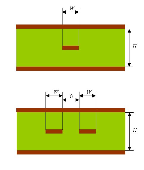
The PCB vendor will need input from you for their calculations. Calculate an estimation of trace widths and spaces using the equations stated below. Make your best guess on how many routing planes you need in the board. List the impedances that your application requires.
A typical substrate to use is FR4. The FR4 substrate have a typical relative permittivity of 4.5 to 4.9.
2. Contact the PCB vendor
Communicate your listings of required impedances, your best guess on the numbers of routing layers and approximated trace widths and spaces with the vendor. From your input they will perform calculations and reply with the accurate figures for your case and for the dielectric they prefer.
3. Finalize layout and routing
Now you are equipped with all the relevant and correct data to finalize carrier board layout and routing.